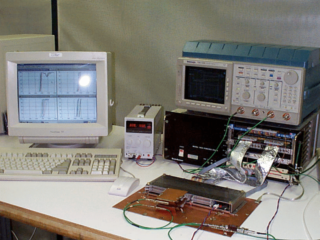
- Minimum (oscillations free) thresholds and noise
(Fig.1) , where:
	Page 1   - thresholds (fC) vs channel # at different Cin
	Page 2   - noise (fC)  vs channel # at different Cin
	Page 3,4 - threshold vs Cin for each channel
	Page 5,6 - noise  vs Cin for each channel
On the pages 1-2 of (Fig.1) the
channels 65-80 are for the first chip and 81-96 - for the second one. Also
though the plot titles say chip 5, chip 6 or chip 3, chip4 (in time resolution
results below), the data were taken for one and the same two chips (3,5 stand
for the first chip and 4,6 - for the second). We are sorry about inconvinience
this can cause, it will be corrected later.
- Thresholds vs JTAG
(Fig.2) , where:
	Page 1-10 - thresholds channel by channel
	Page 11   - thresholds vs channel # at fixed JTAG=180
- Noise vs JTAG
(Fig.3) , where:
	Page 1-10 - noise channel by channel
	Page 11   - noise vs channel # at fixed JTAG. The line 1.0+0.011*Cin
                    is from the chip specification  (Spec.) . Data for chip 6
		    are presented at JTAG=210 because they are not available at JTAG=180.
- Amplifier gain and discriminator level
(Fig.4) , where:
	Page 1-10 show calculation of the gain and discriminator level for each
                  channel. The Ud means the discriminator offset (in mV)
		  relatively to the discriminator level. The Ud is controlled
		  by JTAG. The Thr.(fC) is the threshold at given JTAG. The fit
		  of the first 3 points by the straight line  gives the
		  gain (in mv/fC) and discriminator level as Ud at which the
		  line crosses the Ud axis.
	Page 11 - gain (mv/fC) vs ch # at different Cin
	Page 12 - discr. level (mv) vs ch #  at different Cin

